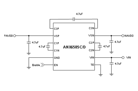
The ANX6585 is a high perfomance charge pump converter to generate positive and negative voltage supply optimized for small to medium size thin-film transistor (TFT) liquid crystal displays (LCD’s).
The positive charge-pump controller provides 2x positive output voltage PAVDD and fixed -1x ratio of negative voltage NAVDD to supply the TFT LCD.
To minimize the inrush current a built-in soft start circuit sets the soft start period.
The ANX6585C performs truly shutdown. It means VSP is 0V when EN is low. The VSP of ANX6585D is pre-charged to VIN when EN is not pulled high. Both ANX6585C and ANX6585D provide the self-discharge function when EN is pulled down.
The ANX6585 is convinient to use and requires only 5 small and low-cost ceramic capacitors. It is availiable in the TDFN-12L package which reduces board size and make the FPC or PCB layout design easier.
l 2.5V to 4.5V Input Supply
l Support x2 Positive Voltage Charge Pump
l Negative Voltage Charge Pump Follow x(-1)
l Positive Output Voltage
l Positive Output Voltage up to +6.0V
l Negative Output Voltage down to -6.0V
l Up to 90% Power Conversion Efficiency
l Up to 120mA Output Current
- 50mA Output Current Capability @VIN=2.8V
- 120mA Output Current Capability @VIN=3.3V
l Build-in Soft-Start to Reduce Inrush Current
l Cycle by Cycle Input Current Limit Protection
l Self-discharge during Power-off
l Truly Shutdown of the Positive Output VSP(ANX6585C)
l Pre-charge the Positive Output VSP to the
l Input Voltage Level (ANX6585D)
l Small 12-pin 2.4mm*1.5mm*0.45mm TDFN Package
l RoHS Compliant and Halogen Free
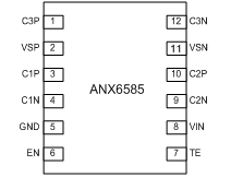
PIN CONFIGURATION (TOP VIEW)
Do Not Sell My Personal Information │Privacy policy │Cookie policy │Terms of use │Terms of sale