HY901 is a smart digital control synchronous rectifier controller functioning as diode emulator. It drives the standard N-channel Power MOSFET to replace Schottky in order to achieve the high efficiency. HY901 incorporates the digital control technology to optimize the multi-mode operation at DCM/PFM/CCM/QR in the different applications. The digital control technology further enhances the robust CCM operation. Adaptive pre-turning off scheme not only guarantees the fast transition but also minimizes switching loss. The adaptive pre-turn off scheme optimizes the EMI due to the soft SR MOSFET switching off transition. The configurable volt-second threshold through INTG pin avoids SR MOSFET mis-trigger transition due to the parasitic ring under DCM/QR mode. HY901 integrates the multi features to minimize the BOM and optimize the performance.
HY901 is available with SOT23-6 package.
· Low-side synchronous rectification without auxiliary winding
· Supports Multi-Mode operation: DCM, CCM, PFM and QR
· Wide output voltage range: 2.8-25V
· Wide VCC bias range up to 8V
· High voltage drain sensing up to 120V
· High current gate driver compatible with various MOSFET
· Driver voltage clamped to 8.0V
· Adaptive pre-turn off driver speeding up turn off transitio
· Selectable option for T_OFF_MIN
· Selectable option for pre-off threshold
· Self-supply to maintain operation with output voltage as low as 2.8V
· Shoot through protection (STP)
· Optimized switching loss and EMI
· Low quiescent current 
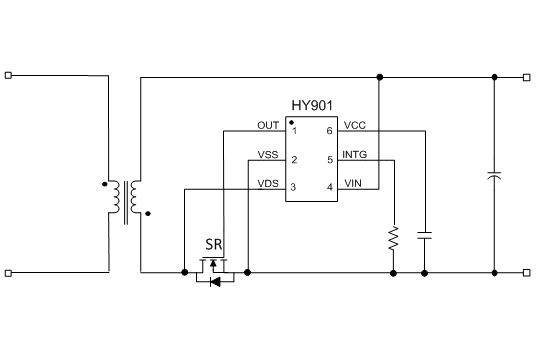
Fig 3. Typical Application Diagram
| Product | HY901A | HY901B | |
|---|---|---|---|
T_ON_MIN | 1.0 μs | • | • |
T_OFF_MIN | 1.25 μs | • | |
2.5 μs | • | ||
| DRV pre-off regulate threshold | -40 mV | • | |
-60 mV | • | ||

Fig 4. Package Diagram
| 標題 | 最後更新 | 分享 | 觀看次數 |
|---|
Pin | Name | Description |
1 | OUT | Gate drive output. Connect OUT with the gate of external MOSFET through a resistor in the application. The PCB trace between OUT and gate of SR MOSFET should be designed as short as possible. |
2 | VSS | Ground. VSS is used as a MOSFET source sense reference. The PCB trace between VSS and source of SR MOSFET should be designed as short as possible. |
3 | VDS | MOSFET drain voltage sense. The PCB trace between VDS and drain of SR MOSFET should be designed as short as possible. |
4 | VIN | HV bias input. VIN pin connected to the converter output voltage. |
5 | INTG | Connect INTG pin to VSS pin through a configuration resistor to setup the integral time after SR MOSFET turns off. This prevents the SR controller from turning on falsely by ringing below the turn-on threshold at VDS pin under DCM/QR mode. |
6 | VCC | IC bias output. VCC is the supply of the HY901. A typical 1uF to 2.2uF X7R bias capacitor is recommended to be designed in applications |
版權所有©2020 華源智信半導體(深圳)有限公司│粵ICP備20068124號